![[METTLER TOLEDO] 분석용 정밀전자저울](http://img.daihan-sci.com/sellerzone_test/banner/-8316562373046649370.jpg)


![[오피스넥스] 종이컵](http://img.daihan-sci.com/sellerzone_test/banner/-6701198976890943434.jpg)
![[오피스넥스] 세계로 지구본](http://img.daihan-sci.com/sellerzone_test/banner/-7788666247607853768.jpg)


- 기준카테고리 : Q
제품설명


상세정보
Perovskite quantum dots (CAS number 15243-48-8) are semiconducting nanocrystals. Compared to metal chalcogenide quantum dots, perovskite quantum dots are more tolerant to defects and have excellent photoluminescence quantum yields and high colour purity. These properties are highly desirable for electronic and optoelectronic applications and hence perovskite quantum dots have huge potential for real world applications including LED displays and quantum dot solar cells.
Highly tolerant
Highly tolerant to defects, retain high PLQY
High purity
99% Quantum Dot Purity
Worldwide shipping
Quick and reliable shipping
Semiconductor
Semiconducting nanocrystals
Caesium lead bromide (CsPbBr3) perovskite quantum dots powder is readily soluble in hexane, octane, and toluene.

Full spectrum range of perovskite quantum dots

The photoluminescence emission wavelength can be tuned by varying the ratio of halides present within the quantum dot, by careful selection the emission can be varied from 400 nm to 700 nm — measurable with the Ossila Optical Spectrometer (see our spectrometer and accessories)
What is a Perovskite Quantum Dot?
A new class of quantum dot is emerging based on perovskites. These have already been shown to have properties rivalling or exceeding those of metal chalcogenide QDs.
Due to their outstanding photovoltaic performance, perovskites are receiving significant attention from the research community. Recently, has been shown that reducing the dimensions of a perovskite crystal down to a few nanometres results in the creation of quantum dots with very high photoluminescence quantum yields and excellent colour purity (i.e., narrow emission linewidths of ~10 nm for blue emitters and 40 nm for red emitters [1]).
These quantum dots are highly tolerant to defects, as they require no passivation of the surface to retain their high PLQY. Although defect and trap sites are present, their energies are positioned outside the bandgap and are either located within the conduction or valence bands [2]. Such perovskite nanocrystals are simple to synthesise in a colloidal suspension and are easily integrated into optoelectronic devices using readily available processing techniques, making them a strong contender for future technologies.
Applications of Perovskite Quantum Dots
Perovskite quantum dots have huge potential for a range of applications in electronics, optoelectronics, and nanotechnology. Currently, the field is not well researched, but initial results are extremely promising. Details on a selection of the applications that have been investigated are given below.
Quantum Dot Solar Cells
Currently, reports of perovskite quantum dot solar cells are still limited, especially when compared to bulk and 2-dimensional perovskites. This is likely due to the limited time that such materials have been available. However, recent results suggest that perovskite quantum dots could play a role in future photovoltaic devices.
Read moreLight-Emitting Diodes (LEDs)
Metal chalcogenide quantum dots already play a role in consumer display products — so the increased PLQY, ease of synthesis, excellent colour purity, and wide colour tunability of perovskite quantum dots suggest that they should be well-suited to such applications. However, charge injection and transport in nanocrystal films must be optimised in order to achieve high-efficiency devices.
Read moreLasers
Amplified spontaneous emission (ASE) has been observed in drop cast films of CsPbBr3, and mixed CsPb(Br/I)3 and CsPb(Cl/Br)3 nanocrystals. Pump thresholds can be as low as 5 µJ cm-2 [13]; a value that compares very favourably with other colloidal QD systems (e.g., an order of magnitude lower than spectrally similar CdSe QDs). The ASE emission intensity is extremely stable in air, dropping by only 10% after several hours of irradiation and ~107 shots in ambient conditions. This performance also compares extremely well to chalcogenide QDs [14]. The stimulated emission has been identified as resulting from the recombination of biexcitons (which are more stable at room temperature than excitons), with red-shifted emission leading to reduced self-absorption (and hence low lasing thresholds). The ASE wavelength can also be tuned throughout the entire visible spectrum via mixing the halide composition.
Read moreSingler Photo Sources
Single photon sources are required for new light-based quantum information systems. Here, current efforts mainly focus on the use of epitaxially-grown quantum dots, diamond colour centers and colloidal nanocrystals. Of these, colloidal NCs are the most promising for room-temperature visible operation [20].
Read morePhotodetectors
The high absorption coefficient of perovskite QDs over a wide spectral range may make them suitable candidates for use in light-detection devices. Pan et al. have reported the fabrication of a phototransistor based on FAPbBr3 quantum dots and graphene [22]. The QDs which act as the light absorber, are deposited onto a monolayer of graphene that transports photoexcited charges to the source/drain. Such phototransistors have a broad response spanning the visible spectrum, although they have reduced response to photons having energies below the semiconductor bandgap (540 nm). Here, a photoresponsivity of 1.15×10⁵ AW-1 was observed at 520 nm; a value that is amongst the highest of any graphene-based photodetectors.
Perovskite Quantum Dot Structure
Halide perovskite nanocrystals have a cubic crystal structure with the chemical formula A+Pb2+X-3. They can be classed as an organic-inorganic hybrid, where A is an organic cation such as methylammonium (MA) or formamidinium (FA), or fully inorganic (A=Cs), and where X is a halogen (Cl, Br, or I). Due to the lack of volatile organics, fully-inorganic nanocrystals tend to have better stability and higher PLQY (>90%) than hybrid organic-inorganic materials [3]. Mixed halide perovskites can also be produced where X is a mixture of Cl/Br or Br/I.
For visible optoelectronic applications, the nanocrystals are generally synthesised to have a size of 4 – 15 nm (dependent on the halogen atom and the required optical properties). The emission wavelength can be tuned through the entire visible spectrum (400 – 700 nm [4]) by changing either the nanocrystal size or halide ratio (for mixed halide systems).

Figure 1: Lead halide perovskite quantum dots have a cubic structure and are often synthesised with organic ligands
Perovskite Quantum Dot Synthesis
The first hybrid organic-inorganic perovskite quantum dot colloidal synthesis of MAPbBr3 was reported by Schmidt et al. using a hot injection method (similar to that used to synthesise metal chalcogenide QDs [4]). A mixture of methylamine bromide and lead bromide was injected into an octadecene solution containing oleic acid and a long chain alkyl ammonium bromide. The PLQY of the resulting QDs was ~20% and was stable for several months due to the stabilising and capping effects of the ammonium bromide and oleic acid. By optimisation of the reactant molar ratios, the PLQY was increased to over 80% [5], and later to ~100% by changing the capping ligand [6].

Figure 2: The synthesis of perovskite quantum dots involves injecting Cs-oleate into a lead precursor.
Hot injection was again used for the colloidal synthesis of inorganic metal-halide perovskite quantum dots, first reported by Protesescu et al [1]. That recipe developed was as follows:
- The caesium precursor Cs-oleate is first prepared by mixing caesium carbonate (Cs2CO3) and oleic acid (OA) in octadecene (ODE), and heating under nitrogen until the Cs2CO3 has reacted with the OA. This solution must be kept above 100 °C to prevent precipitation of the Cs-oleate.
- A lead halide precursor is prepared by mixing a lead halide (PbCl2, PbI2, PbBr2 or a mixture of these) in ODE at 120 °C under nitrogen, along with OA and oleylamine (OLA) that act as stabilising agents. Once the lead halide has dissolved, the temperature is increased to between 140 – 200 °C (depending on the required nanocrystal size).
- The caesium precursor is then injected. After 5 seconds, the mixture is rapidly cooled in an ice bath, with the quantum dots being isolated through centrifuging.
The resulting nanocrystals have surface ligands comprised of OA and OLA [3]. Such nanocrystals were found to have PLQYs up to ~90%, with the smallest crystals (4 nm diameter) having an emission linewidth (full width half maximum) of 12 nm at an emission wavelength of 410 nm, with the largest quantum dots (15 nm diameter) having a linewidth of 42 nm at 700 nm.
During the production process the reaction mixture is quenched by cooling in an ice-water bathMixed-Halide Perovskite Quantum Dots
An advantage that perovskite quantum dots have over their metal chalcogenide counterparts is the simplicity by which their emission properties can be modified. In addition to tuning the emission wavelength during synthesis through reaction temperature (and ultimately, nanocrystal size), it can also be changed post-synthesis through an anion-exchange reaction [7,8]. By mixing a donor halide source such as octadecylammonium (ODA-Y), chloro-oleyalmine-oleylammonium chloride (OLAM-Y) or tetrabutylammonium (TBA-Y) halide (where Y is Cl, Br or I) with a solution of CsPbX3 nanocrystals, the chemical composition of the nanocrystals can be tuned continuously over the range CsPb(X1-Z:YZ), where 0≤Z≤1.
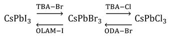
A possible mechanism for anion exchange in perovskite quantum dots
Anion exchange is followed by lattice reconfiguration, giving a mixed halide structure. This results in a single emission peak at an energy somewhere in between those of the constituent nanocrystals, thereby retaining the narrow linewidth needed for color purity. However, it has been found that direct conversion between CsPbI3 and CsPbCl3 is not possible because of the large mismatch in the size of the halide ions.
It has also been demonstrated that this anion exchange process can be easily accomplished by simply mixing different stock solutions of the nanocrystal constituents at different volume ratios (e.g., CsPbBr3 and CsPbI3 to obtain CsPb(Br1-Z:IZ)3 [7,9]). Both methods allow the nanocrystal emission to be tuned over the entire visible range while retaining a high PLQY and color purity. The anion exchange process can however be suppressed by adding polyhedral oligomeric silsesquioxane (POSS) to the solution. This creates a protective cage around the nanocrystals and allows mixing of different halide compositions while retaining the photoluminescent properties of the constituent nanocrystals. It also has the added effect of protecting the nanocrystals from water [10].

Figure 3: A CsPbBr perovskite quantum dot ink under normal illumination (left) and ultraviolet illumination (right)
 CsPbBr
 CsPbBr
 CsPbBr
배송/반품/교환 안내
(1)일반고객, 소비자
- 주문금액 100,000원 미만 : 운임비 고객 부담. 착불 또는 주문시 결제가능
- 주문금액 100,000원 이상 : 운임비 판매자 부담 (단, 택배배송 불가능 상품은 고객부담)
(2)납품업체, 딜러
- 주문금액 100,000원 미만 : 운임비 고객 부담. 착불 또는 주문시 결제가능
- 주문금액 100,000원 이상 : 운임비 판매자 부담 (단, 택배배송 불가능 상품은 고객부담)
택배발송이 불가한 상품, 장비류(Oven, Autoclave, Mill, Cart류 등), Glass Tube, 등의 운임비 별도로 명시된 상품 : 운임비 고객부담
(1)상품배송 완료 후, 14일 이내에 상품에 하자가 없는 경우
(2)포장상태에 이상이 없고, 재판매가 가능한 경우 (단, 왕복 택배비는 고객님께서 부담하셔야 합니다)
(1)반품 요청 기간이 지난 경우
(2)주문 당시 재고가 없어, 해외 발주 상품의 경우
(3)포장을 개봉하였거나 포장 및 제품이 훼손되어 상품가치가 현저히 상실되고 재판매가 불가능한 경우
(4)구매자의 책임 있는 사유로 상품 등이 멸실 또는 훼손된 경우
(5)고객의 주문에 의해 제작되는 주문제작의 경우
(6)반품으로 배송되는 과정 중 파손된 경우 (택배사의 주의 혹은 부실포장으로 인한 파손이므로 반품불가)
(1) 상담센터 (031-217-7950)
(1) 절차에 따라 택배발송 또는 화물 발송.
(2) 수리비 발생시 고객님께 통보, 입금 확인 후 제품 발송
(1) 장비구매시, 구매인증 하신 후 1년
(2) 무상 A/S 불가능할 경우 :
① 장비를 임의로 개조하여 사용하였을 경우
② 주문제작으로 가공된 초자 가공품류(꼭! 상담을 먼저 해주세요.)
거래에 관한 자세한 안내는 구매하신 올포랩 고객센터로 문의해 주시기 바랍니다. (올포랩 : 1661-1179)